Overview Repository OverviewRTL Implementation RTL Verification ASIC Implementation Current Status of Tasks In this proposal, the entire GPS baseband functionality is realized using a combination of custom designed logic functionality GPS Engine (ASIC portion) and the on chip RISCV microprocessor to provide the complete position fix starting from the digitized IF input bits. The signal processing operations in the baseband comprise of dispreading and data demodulation performed on six identical channels followed by psuedo range, and position fix computation. The major part of the signal processing operations for the six channels are carried out in the GPS Engine and the low frequency control tasks and position fix computation tasks are carried out in the RISCV processor.
GPS_Baseband/verilog/rtl/ and GPS_Baseband/verilog/rtl/gps_engine including GPS Engine Modules and user_proj_example and user_proj_wrapper.GPS_Baseband/verilog/dv/. The main testbenches are wb_bfm_carrier_part_test, wb_bfm_goldcode_test, wb_bfm_test.user_proj_example.v , go to GPS_Baseband/openlane/ and run make user_proj_example in the terminal.
The Caravel user_proj_example.v has eight instanciation of GPS channel and a I2C Master . Each GPS Channel has (i) Gold Code generators with the Prompt(P) , Early(E) and Late (L) versions with the latter two being used for the DLL (ii) Number Controlled Oscillators (NCOs) for code clocks for code tracking as well as carrier sine and cosine generation for digital downconversion and carrier tracking (iii) multiple integrate dump filters (accumulators) to perform the correlation operations. and the I2C Master is used to configure the GPS RF Front End chipset .
The following block diagram shows the internal blocks of single gps channel 
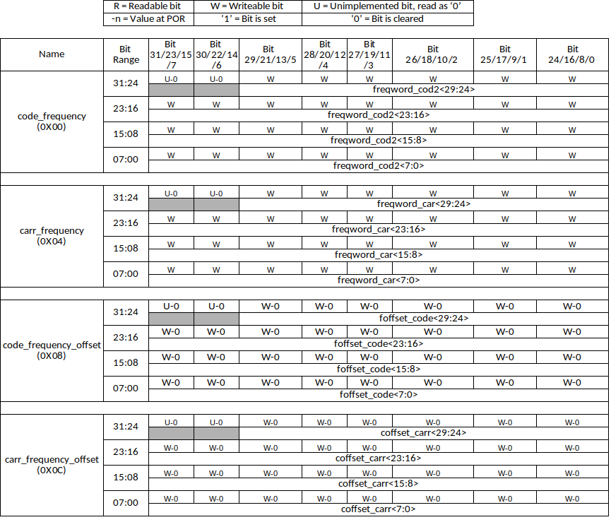
accumulator.v - 20 bit accumulatoradc2to3bit.v - Two to three bit mapping of the input dataclk_gen_gps_new.v - Module containing NCO for Carrier Generation and code clock generationcodectrllogic.v- Topmost module for generation of three versions of Goldcodes (Early,Late,Prompt)codegen.v - Goldcode instantiation modulegoldcode.v- Goldcode generation module based on the Satellite IDgps_multichannel.v - Topmost Module containing 8 single channels and address decodinggps_single_channel.v - Single channel module containing all module instantiations and Wishbone Interfacesignmag_twocomp_vv.v - Sign Magnitude to Two's complement Conversionsignmul.v - 3 bit Sign Magnitude Number multiplierthresh_control.v - Threshold check block to generate Carrier change pulse to invoke Dopplerthreshold.v - Threshold check block to check whether the satellite is acquired or nottrack_intganddump.v - Gold code multiplication with Integrate and dumping of 6 signals(3 - i and 3 - q)wb_interface.v - Provides interface between 32-bit wiishbone bus and internal blocks . Through this wishbone interface , software can write and read memory mapped registers . The details of the wishbone registers is mentioned below .


The verification environment is shown in the following block diagram . A wishbone bus function model is used to create wishbone write and read transactions . The gps raw data is stored to a txt file and being used in the simulation environment .

The following test cases were created and used to verify the gps channel at block level and system level
wb_bfm_carrier_part_test : This test is to verify the working of Carrier generation (cos and sine) at a correct frequency and proper integration and dump of the signals. The Sine Input Text file has the data of 1.405MHz sine wave sampled at 5.714285MHz Clock generated from Matlab. The Local Gold code generation has been forced to 1, so that we can exploit the effects of carrier generation alone. When the sine data is given as input to the RTL and the Local Carrier Frequency is set to 1.405MHz + 100Hz, the I-arm and Q-arm must contain on the the Difference Frequency component, which is 100Hz. Thus, this proves to us that our carrier generation is taken place for a proper frequency, multiplication has taken place correctly and Integrate and dump is also done correctly. The waveform can be seen using the gtkwave viewer and the waves to be seen are gps_engine_i.ch1.tid.dip_track and gps_engine_i.ch1.tid.dqp_track (Can be seen as Analog for Better interpretation)
wb_bfm_goldcode_test : This Testcase is to check the Goldcode generation and creating Half chip delays incase of No acquisition. The Carrier Frequency has been set to 0Hz and the Cosine wave has an amplitude of +1 and Sine wave has an amplitude of 0 throughout the simulation time. The Input Goldcode Text file contains a delayed version of the goldcode data corresponding to Satellite 20. This data has been created using Matlab and fed into the RTL. With Delay we have introduced, an acquistion peak value of around 5000 is expected around 6ms time. This can be checked by viewing the waveform gps_engine_i.ch1.tid.dip_track , gps_engine_i.ch1.tid.die_track , gps_engine_i.ch1.tid.dil_track. From the waveform, we can interpret that the Half a chip delay introduction increases the I arm data and thus acquistion peak is reached. After reaching peak, as we have given the Threshold value to be high for demonstrational purposes, the Delay chipping continues and the peak is not seen in the subsequent epochs.
The testcase can be simulated by executing the following command
.. code:: bash
 cd verilog/dv/wb_bfm_goldcode_test/
 ./verify_gold.sh
.. code:: bash
 cd verilog/dv/wb_bfm_carrier_part_test/
 ./verify_carrier.sh
The Physical implementation of single gps channel is carried out using openlane tool flow with the timing constraint of 50MHz .

